
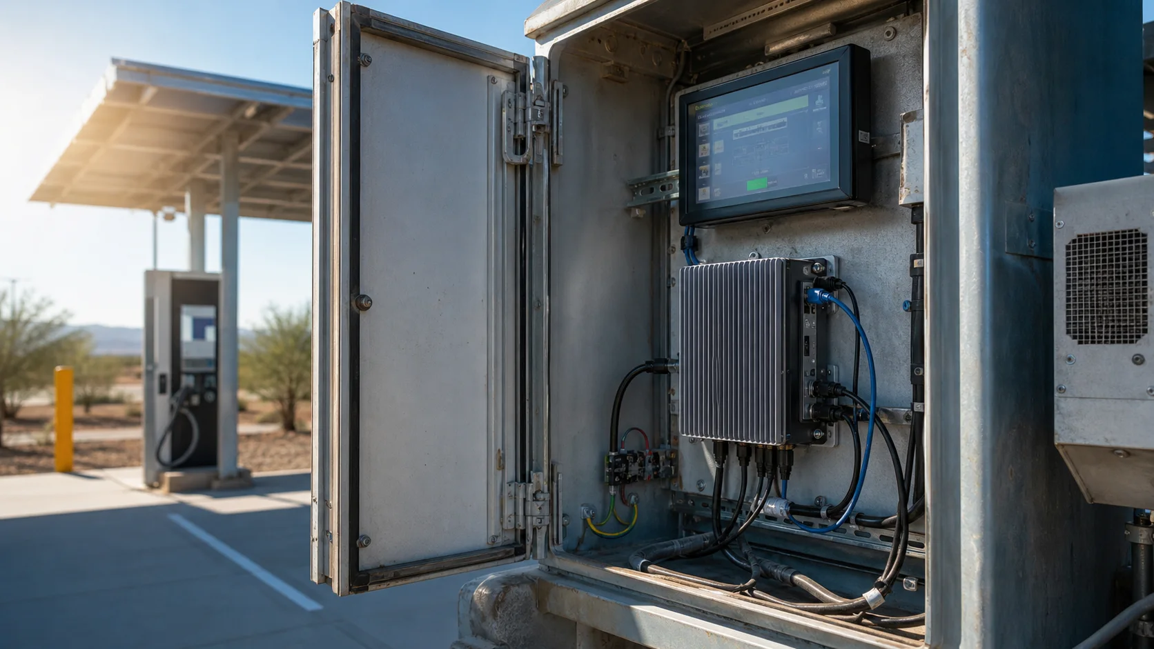
An open Android board can pass a one-hour test and still throttle every afternoon inside a product with a bright display, modem, wall insulation, dust, and sun-warmed glass. Those are different thermal systems.
Thermal design is not choosing a heatsink from a catalog. It is defining where heat is generated, giving it a repeatable path to ambient air, and verifying that Android maintains the required workload without unacceptable throttling or surface temperature.
Start with the real power map
Processor TDP is not a product power map. Measure the SoC, memory, PMIC, backlight, storage, wireless, power conversion, and peripherals. A 6 W SoC beside a 10 W backlight driver can move the hotspot away from the processor.
Use the production APK and resolution. Combine animations, video, inference, database writes, and network traffic realistically. CPU stress is repeatable but misses GPU, NPU, memory, and display paths. Keep both a sustained product workload and a harsh guardband test.
The Android SBC power-budgeting guide is a good starting inventory. For thermal work, add where each watt is dissipated and whether it has a useful path to the enclosure.
| Heat source | What raises its dissipation | Common integration mistake |
|---|---|---|
| SoC and memory | UI resolution, CPU/GPU/NPU load, memory bandwidth | Testing only CPU stress on an open board |
| Display/backlight | Brightness, panel efficiency, LED-driver loss | Ignoring heat trapped behind the LCD |
| PMIC/DC-DC | Input voltage, current, conversion efficiency | Placing the hot converter beside the SoC |
| Wi-Fi/LTE modem | Transmit duty cycle and poor signal | Testing near an access point only |
| eMMC/NVMe | Sustained writes and garbage collection | Short benchmark before steady state |
| USB peripherals | Device load and internal regulator loss | Adding peripherals after enclosure freeze |
Give heat a deliberate route
For a sealed product, convection around a tiny board heatsink is limited. The most useful path often runs from SoC package to thermal interface material, to a heat spreader or enclosure boss, through the metal chassis, and finally to ambient air. Each interface adds thermal resistance.
A first-order model is Tj = Ta + P × θ. It is a planning tool, not proof; effective resistance changes with the PCB, interface compression, orientation, airflow, nearby sources, and mounting surface.
Texas Instruments’ thermal design guide for ARM application processors makes the same practical point: data-sheet theta values are based on defined test conditions and do not replace modeling and system testing. Use calculations to compare concepts, then measure the assembled product.
For top-side conduction, control these details:
- package-to-spreader gap across component and PCB tolerances;
- thermal pad conductivity, thickness, compression range, and long-term set;
- spreader flatness and mechanical load on the PCB;
- insulation from nearby tall or sensitive components;
- assembly method that operators can reproduce;
- creepage, clearance, and grounding requirements for the enclosure.
A thick, soft pad can absorb tolerance but adds thermal resistance. A thin pad performs better only when the stack-up can guarantee contact. Thermal paste may look excellent in a prototype and become a production mess. Pick a material the factory can inspect.
Use the PCB and enclosure together
Heat leaves an SoC through the package top and through the soldered board. Copper planes, thermal vias, and component placement affect the bottom path. Do not place the Wi-Fi module, eMMC, and main regulator in the same stagnant pocket simply because routing is convenient.
An aluminum enclosure is both a spreader and a radiator. External fins help only when their orientation and surrounding clearance support air movement. Fins pressed against a wall or hidden inside a flush mounting recess add less value than the CAD image suggests.
Plastic products need a different strategy: internal aluminum spreader, graphite sheet where appropriate, controlled vents if the ingress rating allows them, and distance between the heat source and user touch surfaces. A decorative metal front bezel can unexpectedly become the hottest touch point.
Android thermal behavior must match the hardware
Android does not merely report a CPU temperature. Its thermal framework coordinates sensors, throttling severity, cooling devices, applications, and shutdown. The current Android thermal mitigation documentation specifies Thermal HAL 2.0 and notes that Android 14 moved the interface from HIDL to AIDL.
Verify the BSP. Sensor names must map to physical locations, throttling states and frequency limits must take effect, severity must be reported, and shutdown must precede hardware limits. A temperature node alone is not a finished policy.
Use dumpsys thermalservice, kernel thermal zones, frequency statistics, workload metrics, and external thermocouples together. The on-die sensor explains junction behavior. It does not tell you whether the glass where a user rests a hand is too hot.
Do not disable thermal mitigation to win a benchmark. If the product cannot meet its workload with the policy enabled, change the thermal path, workload, or platform.
Define pass criteria before the chamber test
“It did not shut down” is a weak thermal requirement. Set limits for sustained frame rate or transaction time, allowed frequency throttling, enclosure touch temperature, display and storage temperatures, application behavior at each Android thermal severity, and recovery after ambient temperature falls.
| Test condition | Measurements | Example decision question |
|---|---|---|
| Room ambient, nominal workload | Baseline power, temperatures, frequencies | Is the assembly behaving as modeled? |
| Maximum rated ambient | Junction proxy, case, display, PMIC, storage | Does the product sustain its required task? |
| Poor radio signal | Modem duty cycle and local hotspot | Does cellular transmit create a new limit? |
| Maximum backlight | LCD rear surface and front touch temperature | Is outdoor readability thermally sustainable? |
| Enclosure orientation variants | Hotspot and time to steady state | Does wall mounting block convection? |
| Recovery after soak | Temperature and performance vs time | Does throttling release without reboot? |
Use a thermal chamber where possible, but do not let chamber air blow directly across vents in a way the installation never will. Add insulation or mounting fixtures that represent the wall, cabinet, or console. For outdoor products, include solar loading or an equivalent controlled heat input.
Wait for steady state. Plot temperature over time and stop when the slope is acceptably small, not after an arbitrary ten minutes.
Investigate contact, not just temperature
When units differ, inspect the stack with pressure film, pad witness marks, disassembly photos, and gap measurements. Infrared finds hotspots, but shiny metal has variable emissivity; use known-emissivity tape or contact sensors for quantitative readings.
Route fine thermocouple wire consistently and photograph every location. “Sensor near the CPU” cannot be reproduced.
Check units after vibration and thermal cycling. Screws relax, pads take a compression set, adhesives age, and an enclosure can warp. A prototype that relies on hand-adjusted pressure is not ready for production.
Tune software after fixing the heat path
Software can cap unnecessary peak frequency, move synchronization outside active UI periods, lower idle camera rate, and avoid rendering invisible frames. Let the application drop optional work first as Android thermal severity rises.
But software tuning should not hide bad contact or an undersized enclosure. Repeat the same workload before and after each change. Track energy per completed task, not only peak temperature. Finishing a job faster at higher power can sometimes generate less total heat than running slowly for longer.
This work also feeds Android board lifecycle planning. A supplier’s memory substitution or enclosure paint change can alter thermal behavior. Keep the validated hardware and material stack in the release record.
Frequently asked questions
What is a safe Android SBC temperature?
There is no universal number. Use the SoC and component operating limits, Android thermal policy, touch-temperature requirements, enclosure material, and product environment. Design below absolute limits with measured margin.
Is a thermal camera enough for validation?
No. It shows surface patterns and is excellent for diagnosis, but emissivity can mislead readings and it cannot directly measure semiconductor junction temperature. Combine it with calibrated contact sensors and on-device telemetry.
Can a fanless enclosure support an RK3588-class workload?
Possibly, if the sustained workload, ambient, enclosure area, conduction path, and throttling target line up. The SoC name does not answer the question. Build and soak the complete assembly.
The practical standard
A good fanless design reaches a predictable steady state, holds the required workload, keeps touch surfaces and components within their limits, and recovers cleanly from throttling. It does so across assembly tolerance, orientation, ambient range, and product workload.
If the conclusion depends on one open-board benchmark or one infrared image, the thermal design is still a hypothesis.
Primary references
- Android Open Source Project: Thermal mitigation
- Texas Instruments: Thermal Design Guide for DSP and ARM Application Processors