
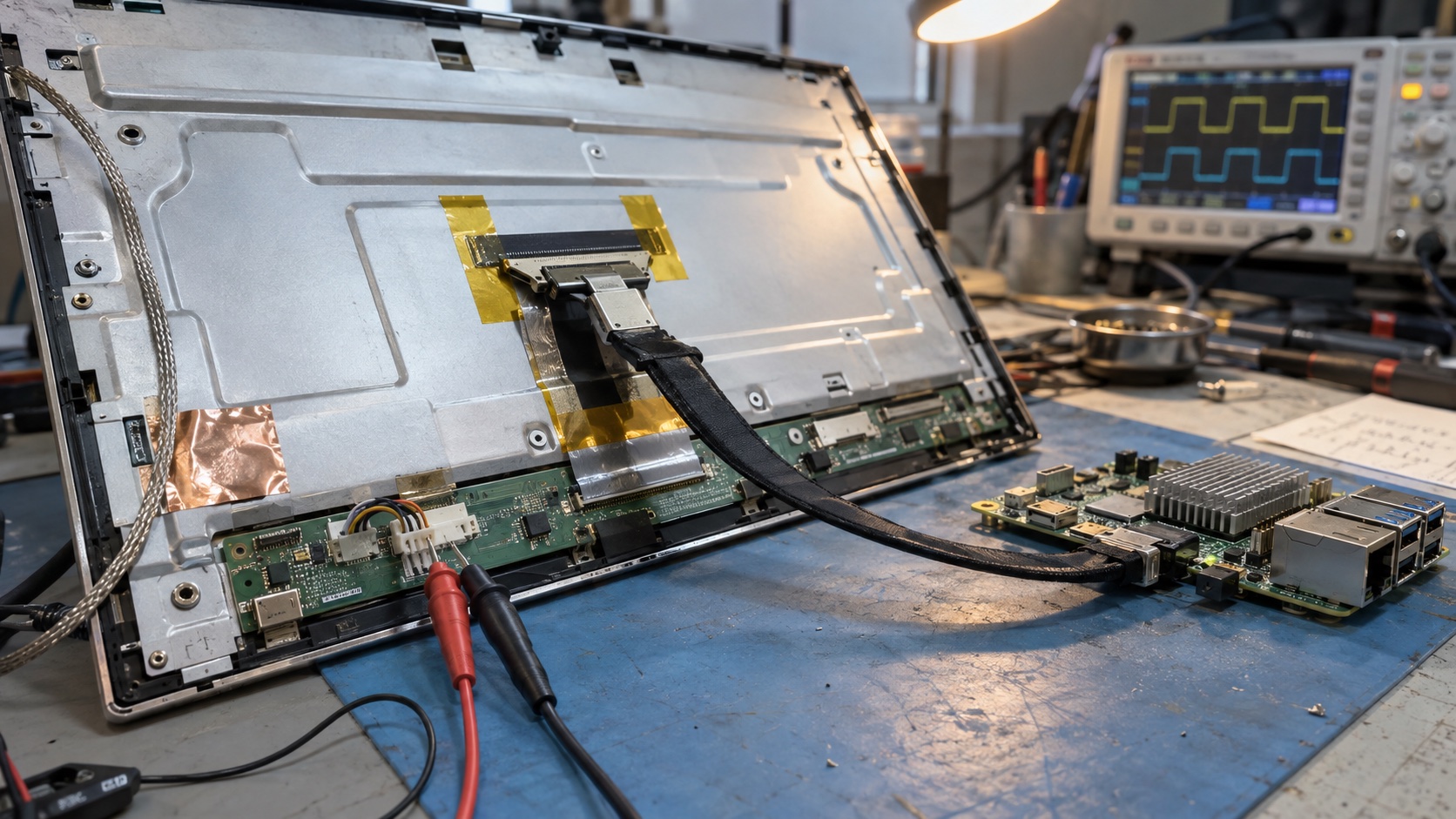
An eDP panel can stay black even when the link is training correctly. The backlight may be off. Panel power may arrive in the wrong order. The AUX channel may work while the video lanes do not. And a display sold under the same marketing name may change timing controller between production lots.
That is why eDP bring-up should be split into power, discovery, link training, video timing, and backlight. Debugging “the display” as one block wastes days.
What eDP changes in an Android SBC design
Embedded DisplayPort is a packetized digital display link intended for internal panels. It commonly carries video over one, two, or four high-speed lanes and uses an AUX channel for configuration and panel capability exchange. Hot-plug detect, panel power, reset or enable signals, and backlight control still need board-level attention.
Do not treat the connector as a small HDMI socket. Pin assignments, voltage rails, lane count, lane polarity options, AUX routing, backlight power, and cable construction are panel-specific.
| Signal group | Purpose | Typical integration error |
|---|---|---|
| Main link lanes | High-speed video transport | Wrong lane mapping, poor impedance, excessive loss, or unsupported rate |
| AUX pair | Configuration, training, and panel communication | Pair swapped, wrong pull network, or noisy routing |
| HPD | Reports panel presence or readiness | Floating level or incorrect voltage domain |
| Panel logic power | Runs the timing controller | Rail value or sequence copied from a different panel |
| Backlight power | Supplies LED driver or panel backlight stage | Connector current and inrush underestimated |
| Backlight enable/PWM | Turns light on and controls brightness | Active polarity or PWM frequency assumed |
The first decision is whether the SoC and BSP expose a native eDP controller with production support. A bridge from DisplayPort, HDMI, MIPI DSI, or LVDS can work, but it adds clocking, power sequencing, firmware, and failure modes. Native is usually the cleaner path when the exact panel is supported.
Freeze the panel identity before routing
Obtain the full panel specification, not a reseller summary. Record the exact model and revision, native resolution, pixel format, lane count, supported link rates, logic and backlight rails, maximum inrush, connector part, mating orientation, mechanical keep-outs, and timing requirements.
Panel sourcing belongs in the electrical review. Two 13.3-inch 1920 × 1080 panels can use different connectors, backlight voltages, or link capabilities. A supplier-approved “equivalent” is not equivalent until it passes the same integration tests.
Ask for the panel’s power sequence and timing limits. Some panels require logic power to stabilize before HPD or AUX activity; others specify delay from link readiness to backlight enable. Sequence violations can appear as a cold-boot-only fault, which is why bench reboots often miss them.
For other internal display options, compare the practical constraints in the LVDS display guide and MIPI DSI integration guide. The interface decision should include cable length, panel availability, EMI, BSP support, and future replacements.
Route the main link as a high-speed channel
Use the SoC, connector, and panel layout guidance together. Keep each differential pair impedance controlled, minimize discontinuities, and avoid unnecessary vias or stubs. Lane-to-lane length requirements are not permission to serpentine aggressively; added meanders create loss and coupling.
Route AUX as a differential pair even though it runs far slower than the main link. Keep it away from switching nodes and noisy backlight power. Give HPD a defined level and confirm the input voltage domain.
The cable is part of the channel. Specify length, impedance, conductor arrangement, shield termination, bend radius, and mating life. A thin prototype cable draped across a bench does not represent a cable folded behind a metal panel and tied beside the backlight converter.
Grounding deserves a mechanical drawing. Decide how the panel frame, cable shield, SBC ground, and enclosure meet. Accidental contact through one mounting screw can make prototypes inconsistent and create radiated-emissions surprises later.
Build the power and backlight sequence deliberately
Separate the panel logic rail from backlight power in the test plan. Measure both at the connector with the panel attached. Backlight startup can draw enough current to dip a shared rail even when average consumption looks safe.
Use an oscilloscope to capture panel power, HPD, AUX activity, backlight enable, and PWM during cold boot, warm reboot, suspend, and resume. A logic analyzer can help with discrete control timing, but it will not show a marginal rail.
Many eDP panels support AUX-controlled brightness, while others rely on a board PWM and enable pin. Linux display drivers may select a native AUX backlight path when the panel advertises it; vendor Android BSPs sometimes keep a board-specific PWM implementation. Confirm which path is active instead of changing brightness tables blindly.
For visible banding or poor low-level control, inspect PWM frequency, polarity, duty-cycle limits, and the LED driver response. The backlight and power budgeting guide helps capture the load, but display quality still requires a luminance measurement across the brightness range.
Debug a black panel in layers
Start with evidence. Do not change device tree timings, cable, and power sequence at the same time.
| Observation | Likely area | Next measurement |
|---|---|---|
| No HPD and no AUX traffic | Power, connector, HPD wiring | Panel logic rail and HPD level at both ends |
| HPD present, AUX fails | AUX routing or voltage | Pair continuity, polarity, bias, and waveform quality |
| AUX works, training fails | Lane map, rate, loss, or panel capability | Driver logs, negotiated lanes/rate, channel inspection |
| Training succeeds, no image | Timing, pixel format, compositor path | DRM state, frame activity, test pattern |
| Faint image under a flashlight | Backlight path | Backlight rail, enable, PWM, and driver current |
| Works warm, fails cold | Sequence or marginal power/channel | Cold-start rail and signal captures |
| Random sparkles or dropouts | Signal integrity | Cable substitution, reduced rate, lane error data |
Confirm panel power and current first. Then read HPD, check whether AUX transactions occur, inspect kernel or DRM logs for discovered capabilities, and verify the negotiated lane count and link rate. Only then move to display mode and Android composition.
Reducing the link rate or resolution can be a useful diagnostic. If the panel becomes stable, the channel may be marginal. It is not a production fix unless the reduced mode still meets the specification and passes temperature, cable, and emissions testing.
Verify the Android display stack
On Android, a trained eDP link can still produce a blank or unstable UI if the DRM/KMS driver, Hardware Composer integration, framebuffer format, orientation, or density configuration is wrong. Separate a kernel test pattern or simple DRM mode from the complete Android UI when the BSP allows it.
Check that the reported mode matches the physical panel. Verify refresh rate, active resolution, color depth, rotation, and overscan assumptions. Then test boot animation, launcher, video playback, GPU-heavy UI, sleep/wake, and repeated hot or cold restarts.
Touch is a separate subsystem. A panel image does not prove the USB or I2C touch controller will resume correctly or map coordinates after rotation. The touchscreen integration guide provides the matching validation steps.
Qualify the complete assembly
Run link and image tests with minimum and maximum cable lengths, production hinges or bends, target enclosure, maximum backlight, and temperature extremes. Add ESD and radiated-emissions work after the basic design is stable.
Keep golden samples of the panel, cable, and board. When a future lot fails, swap one element at a time and compare panel identifiers and link logs. This is much faster than reopening the entire software stack.
Your release record should include the exact panel revision, cable drawing, device tree or firmware mode, power-sequence capture, brightness curve, and pass criteria. If purchasing changes the panel, rerun the record rather than relying on resolution alone.
Frequently asked questions
Does eDP carry touch data?
Usually no. Touch commonly uses USB or I2C through separate pins or a separate cable. Confirm the display assembly pinout instead of assuming the touch controller shares the eDP link.
Can any eDP panel work with an Android SBC?
No. The source must support the required lane count, rate, timing, and power controls, and the BSP must drive that source correctly. Connector compatibility alone proves very little.
Why does the panel work after reboot but not after cold power?
Cold-only failures usually point to sequencing, rail ramp, HPD timing, or a marginal link that behaves differently with temperature. Capture the first startup rather than attaching probes after the failure.
Bottom line
Successful eDP integration comes from treating the panel, cable, power sequence, high-speed link, backlight, and Android display stack as separate testable layers. Freeze the exact panel, measure every startup signal, and qualify the assembled channel. A stable picture on one warm bench unit is the beginning of validation, not the end.